Amp4 - Subwoofer - Amplifier
In designing the amplifier to drive the horn I have looked for something different to the boring, standard three-stage topology. The final design is a symmetrical folded cascode (technically a folded cascode is one stage, + output stage = two stages in total). Power output is around 25W into 4Ω, which is plenty given that the chosen speaker design is a horn with a predicted 110dB sensitivity. The high sensitivity does demand that noise/hum be kept at an absolute minimum. Although it only needs to have a bandwidth up to ~125Hz, I have still designed it as a full-range amplifier, just because.
With the MOSFETs I'm using for the output stage, there is some benefit to rail efficiency by using a lower voltage supply for the output stage. Thus the output stage gets ±15V (from "PSU2"), everything else gets ±20V (from "PSU1").
Schematic
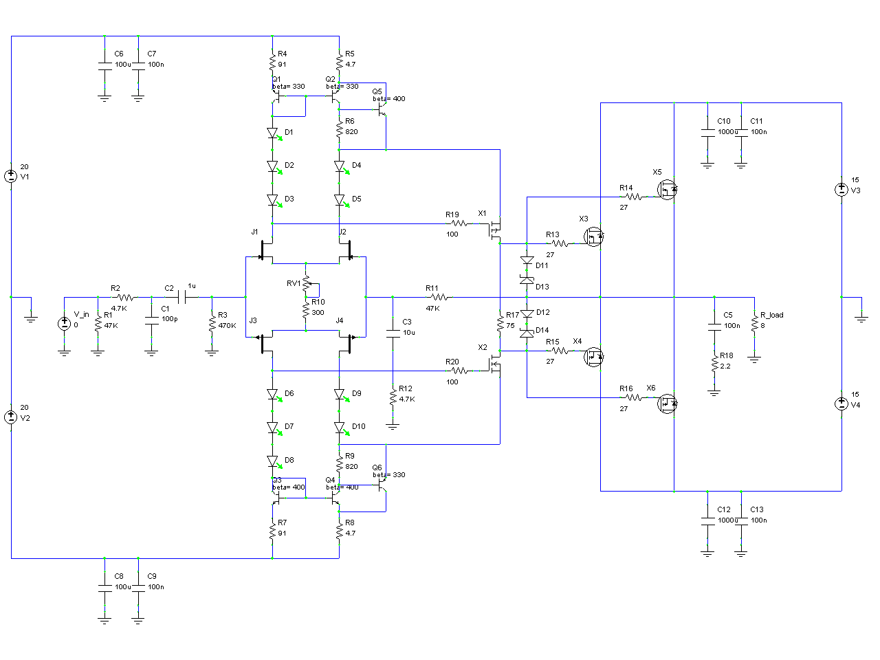
Starting at the beginning: R1 sets the input impedance, then R2 and C1 form a low-pass filter at 339kHz to keep RF out. C2 and R3 form a high-pass filter to block DC.
The input stage is a complementary long-tailed pair. JFETs were chosen here for high input impedance, low input bias current, the ability to forgo current sources for biasing (because JFETs are depletion mode devices) and also partly because I just like FETs and have finally found somewhere that sells 2SK389 and 2SJ109 monolithic dual JFETs (Dalbani, to be precise). The long-tailed pairs are loaded with current mirrors with gain. The ratio of current is a function of the ratio of R4/R5 (and R7/R8) The 'extra' current goes to the cascode. Bias current for the LTP, and thus the whole amp, is set by RV1.
The bias voltage for the cascode stage comes from the strings of three LEDs (D1/D2/D3 and D6/D7/D8). These LEDs are in the LTP to avoid the need for current sources for them. This keeps things as compact as possible, and shaves a few volts off the maximum voltage across the JFETs, allowing them to stay within their ratings even if I were to use higher supply voltages. The strings of two LEDs in the other side of the LTPs also reduce the voltage across the JFETs, but their main function is to limit the gate-source voltage in the cascode MOSFETs in case of a short circuited output.
MOSFETs were chosen for the cascode stage for high input impedance (vital to avoid drawing current from their bias voltages in the LTP) and higher possible output voltage swing. This is the first time I've used small-signal MOSFETs for anything, which makes it particularly interesting for me to see how they perform (and they had better do good, because they're too expensive to waste!). The particular MOSFETs I chose are ZVN2106A/ZVP2106A. They aren't the ideal choice because their power rating is only just sufficient for running at 20mA whereas I would have liked to run them at a higher current to improve the speed they can drive the output devices. There don't seem to be any medium power MOSFETs that aren't also slow though, so they are the best compromise and do seem to be very nice devices otherwise. R19 and R20 form low-pass filters with the input capacitance of the MOSFETs, ensuring stability. They aren't really needed, but they do no harm and it's better to be safe.
R17 provides the bias voltage for the output stage. A simple resistor is sufficient here due to the negative temperature coefficient of the lateral MOSFET output devices. Overall the amp is thermally stable, although it does take some time (about 15 minutes) to reach the final quiescent output stage current from the initial, lower current. Theoretically there would be an improvement to high frequency response by using a voltage source here instead, or at least bypassing the resistor with a capacitor, but the simulations showed only a miniscule difference and measured performance shows no deficiency.
The output stage is a plain old source-follower using two parallel pairs of ECX10N20/ECX10P20 (Exicon MOSFETs, which in my opinion are the best for audio). I prefer MOSFETs for output stages due to their near-indestructibility and (sort of) easy drive requirements, and in the case of lateral MOSFETs (which these are), also negative temperature coefficient, which vastly reduces concerns about thermal stability, simplifying biasing (in many cases, such as here, just a resistor will do). There is no real need for two pairs of devices given the low power output, but there is a minimum order of two on them and it does lower output impedance a bit. Gate stopper resistors are included to prevent oscillations. VGS is limited by the Zener diodes. This not only prevents the VGS limit from being exceeded (which will damage the MOSFETs), but also limits output current in the case of a short-circuit for at least long enough for a fuse to blow, preventing damage to the output devices.
Negative feedback network consists of R11/R12, and C3 which reduces DC gain to unity. The Zobel network across the output (C5 and R18) provide a low-impedance termination for high frequencies, helping to ensure stability, especially into difficult loads.
PCB layout
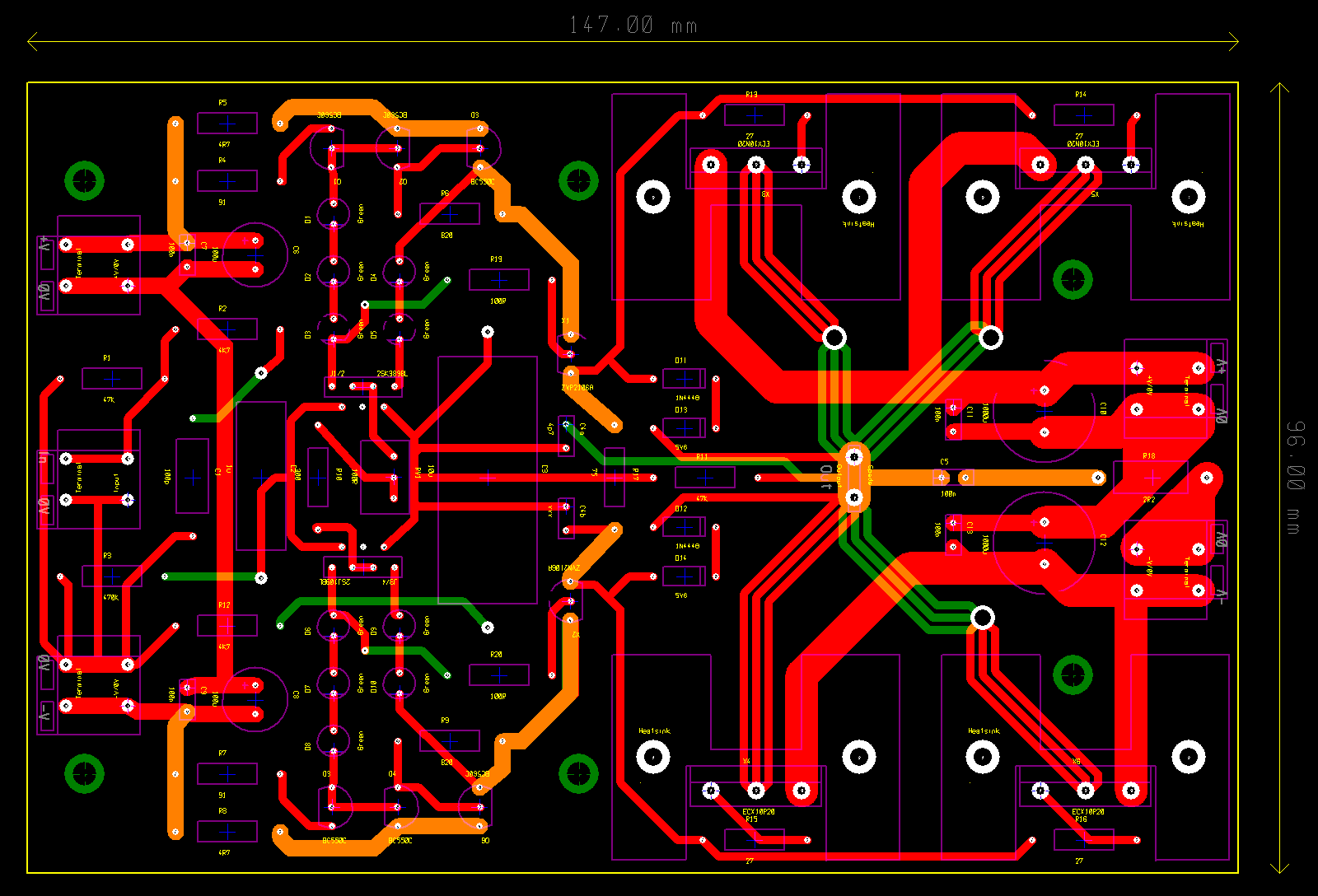
Transistor packages with the gate/base as the middle pin are a real boon. They allow the PCB layout to be much closer to the schematic, which reduces the probability of me making a mistake. The input stage is all on the left. It has two grounds: One power ground and one analogue ground. Keeping them separate is essential to avoid injecting noise and hum via the finite impedance of the tracks and wiring. A few of the tracks which carry the highest currents are duplicated on both sides of this double-sided board (they appear orange). None of them really carry enough current for this to be much benefit, but the copper there would otherwise go to waste, so double-tracks it is.
There is space for two feedback capacitors not shown on the schematic. According to the simulations it is necessary to do something to limit high frequency response so that no ringing is visible with a square wave input, but the prototypes I tested on a breadboard needed none. I have thus left space for some just in case.
The output stage is all on the right. The output devices' heatsinks are PCB-mounted since this is cheaper than buying a single huge heatsink to mount all the transistors on. They are mounted at the edge of the board for maximum airflow. I've been careful to not route any tracks directly under them on the component side since they will not be insulated from the output devices and I wouldn't want anything shorted out.
Note the triple-track from each output device to the output. This minimizes the inductance of these tracks, which is important to reduce the probability of oscillations when paralleling MOSFETs. The Zobel network's tracks on the centre-right of the board are doubled (one on each side of the board) for the same effect. This is because the Zobel network should present a low impedance to high frequencies. For this reason it should also, ideally, be run directly from the output of the amp to the point where the speaker is grounded, which is why it has its own ground connection on the PCB, separate from power ground.
Building and testing
Matching of the transistors in the current mirrors affects DC offset, so I measured hFE of a bunch of them and chose the closest pairs. The JFETs are already matched, being made on the same lump of silicon, so no measurements needed there. There would be some benefit to matching the output devices for the most even current sharing, but it would be expensive to buy enough to do that and they're already pretty close.
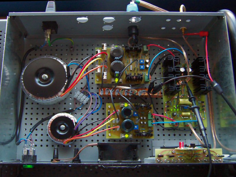
Here's a photo of it all assembled:
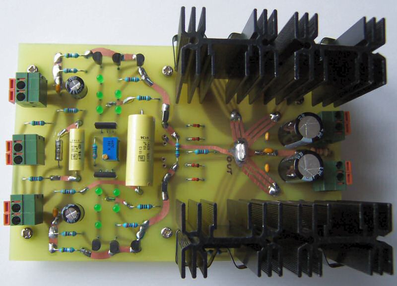
Those green and orange PCB terminals are lever-operated. They're much nicer than the more common screw one; it's easier to insert/remove wires, and they feel to be held more securely. I think I'll avoid screw-terminals completely from now on. Also note the huge yellow polypropylene capacitors. I still have a bunch of them left over from a previous project. Although huge, they beat electrolytics (yes, I do seem to have this phobia of electrolytic capacitors).
On first switching it on I thought something had gone wrong, since the LEDs didn't all light up and there was a low-level oscillation on the output. Probing with the multimeter showed that one supply rail was very low. This was a bit confusing because it went back up to normal level when disconnected from the amp. Eventually I tracked it down to a partially blown fuse, which had a high-ish impedance, not completely open-circuit. I'm not quite sure how it managed to get into that state. After replacing it everything worked fine. Ahhh! Building stuff that doesn't explode is nice :) A few tests with an old speaker and an oscilloscope confirmed that everything was operating as predicted.
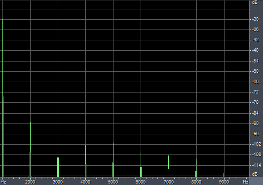
Below is an FFT showing measured harmonic distortion, 1kHz@7Vrms into 8Ω. This represents a THD of about 0.004%.
Slew rate is around 100V/μs
As for listening tests: One of my objectives has been achieved splendidly - the thing is deathly quiet with no input: No matter how close I hold my ear to the speaker I can't hear a thing from it, and I can't measure any noise on the output as it is below the noise floor of my 'scope. After testing with a number of speakers I would have to say I'm happy. It sounds at least as good as any other amp I've ever heard. The only problem is fairly loud turn-on and off thumps. Perhaps a relay between the amp and the speaker would be a good idea.