Useful Components
An exercise in making very small things by hand using SMT components. They have been created to simplify circuit layouts by allowing common circuit functions to be accomplished with small devices with the minimum number of pins. They are great for prototyping.
JFET current source
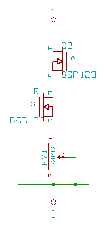
Junction FETs are naturally suited to making current sources; just connect the source to the gate, and magically a constant current flows between source and drain over a wide range of voltages. Commercially available "constant current diodes" are a simple JFET connected like that. Connecting a resistor between source and gate reduces the current, and if it's variable then so can the current be varied, which is just what is needed here. Furthermore, I added a second JFET to cascode the current source. This increases the output impedance and improves high-frequency performance.
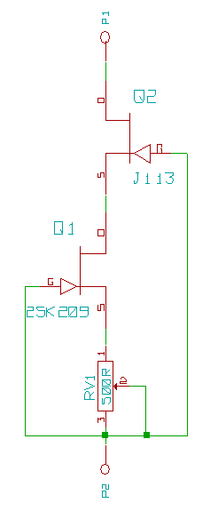
The particular JFETs used here are just ones I happened to have lying around, not necessarily the best possible choices. The cascode JFET must have a higher Idss than the current source JFET in order for it to remain biased on at all output currents. With the transistors and potentiometer value used here, output current can be varied from about 0.5-3.0mA.
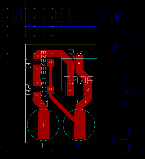
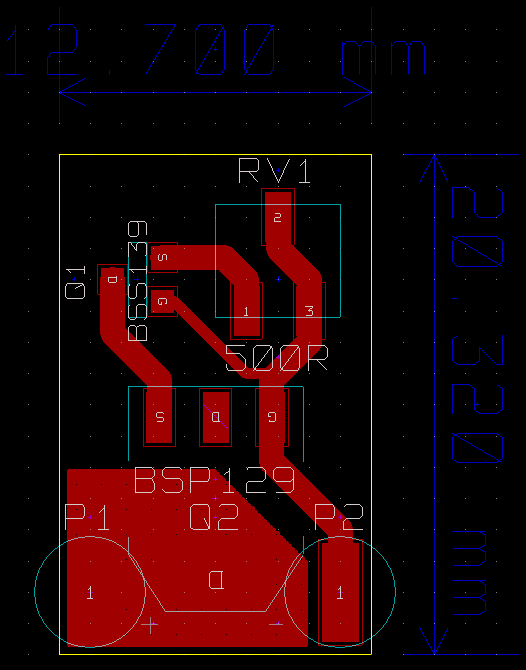
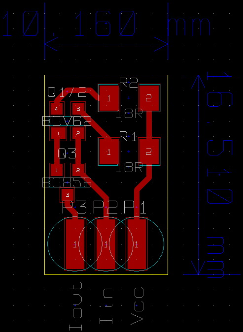
The PCB layout is very simple with only threee components; just a tiny piece of single-sided board needed.
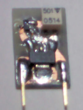
These are two-terminal devices, so they can be used as either current sources or current sinks. Very handy
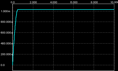
Above is a graph of a simulation of current against voltage. It requires about half a volt across it before it starts to work, then the output impedance reaches several tens of megohms. I measured real performance to be a little worse than that, but not much.
MOSFET current source
Depletion mode MOSFETs work very much like JFETs (which are also depletion mode devices) and can therefore be used to make the same sort of current source. They tend to have higher Idss than JFETs and also massive voltage ratings, making them more suited to high-power applications than the usually wimpy JFET.
The cascode transistor (BSP129) has almost the entire voltage dropped across it, which means that it dissipates almost all the power, allowing a smaller, cheaper transistor (BSS139) to be used for the current source. There aren't many depletion-mode MOSFETs available, so there isn't much else to base a choice on. Output current range is approximately 3-50mA with these components.
Another very simple PCB layout, although slightly larger to accomodate the SOT-223 packaged MOSFET. I have maximized the area of copper that the drain of the cascode transistor is attached to, to aid cooling.
BJT current mirror
I bought some complementary matched pairs of BJTs (BCV61C and BCV62C) a while ago which are internally connected as current mirrors. Obviously this makes them ideal for making... current mirrors. They can be used just as they are, but a few extra components improves the performance. Specifically, emitter degeneration resistors reduce the effects of any mismatch between the transistors, and a third cascode transistor improves output impedance, i.e. a "Wilson" current mirror.
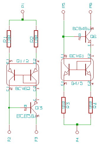
Unlike the current sources, these mirrors care about polarity, so NPN transistors must be used to make a negative current mirror and PNP transistors to make a positive one.
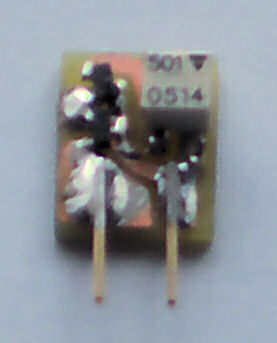
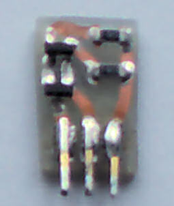
The components are very small, but it's quite possible to solder by hand.
Unfortunately, while the current mirror pairs of transistors are in the C gain group, the cascode transistors are unsorted and turned out to have much lower hfe than the mirror pairs. This means that there is a bit of gain-error, but that is not important for most applications and would be easily fixed by using better matched transistors.
MOSFET current mirror
This one didn't work out so well, but it might still be informative: Dual MOSFETs are quite common and could make a better current mirror than BJTs for some cases due to working with output voltages to within only a few millivolts of the rail.
The output impedance should be higher than for a BJT mirror, so I didn't bother with a cascode transistor.
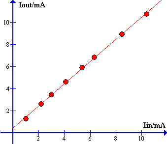
This is a graph of measured output current against input current, which shows the relatively large offset of almost half a milliamp due to poor Vgs matching between the two transistors. Since most circuits that are likely to need a current mirror will operate with currents of the order of 1mA, this is too much. Larger degeneration resistors would help, but would nullify the advantage of wide output voltage swing. Dual MOSFETs never specify how good the matching is, so other devices might be better, but I doubt it.
Diamond buffer
Quite a lot of my experiments in amplifier design involve variations in the input or voltage amplifying stages. Having a standard output stage helps when comparing such designs. For this, a diamond buffer is ideal, offering a high input impedance and low distortion. Good though the standard diamond buffer may be, it can be made even better with a simple modification, as you can see in the schematic.
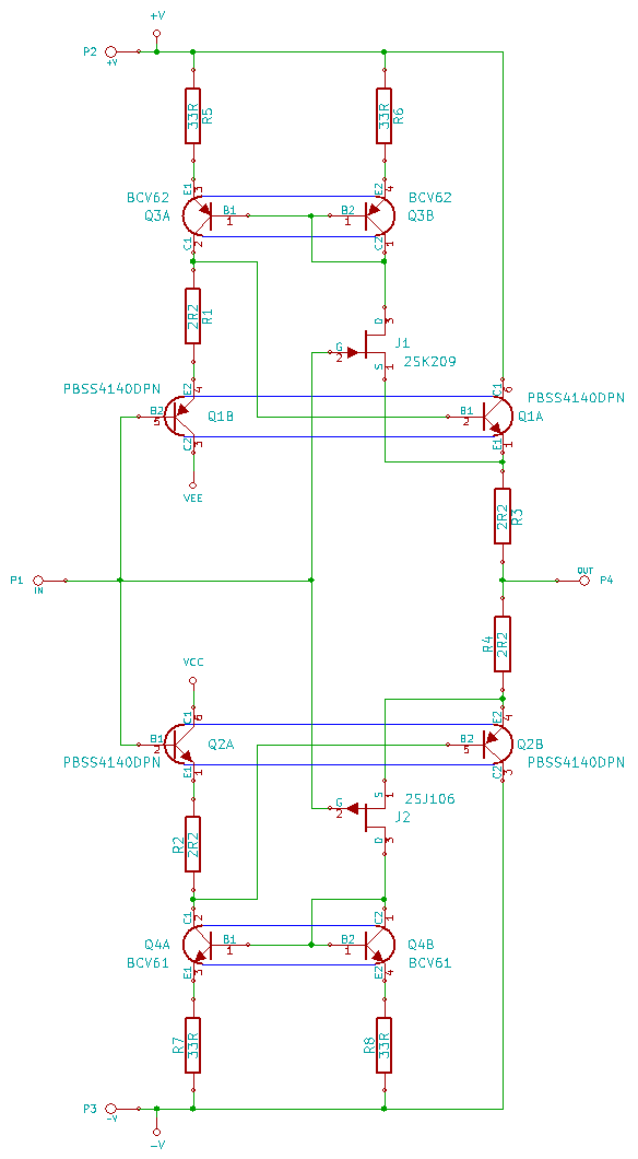
Diamond buffers are commonly biased by a single JFET connected as a current source. The modification here is to add a second JFET and configure the pair as a source-follower in parallel with the diamond buffer. The input voltage to this source-follower is then the difference between the diamond buffer's input and output voltages. This causes the bias current to increase when the load increases, helping to reduce distortion.
You can also see from the schematic that I have chosen to use monolithic pairs of transistors everywhere. This improves temperature stability by keeping pairs at the same temperature.
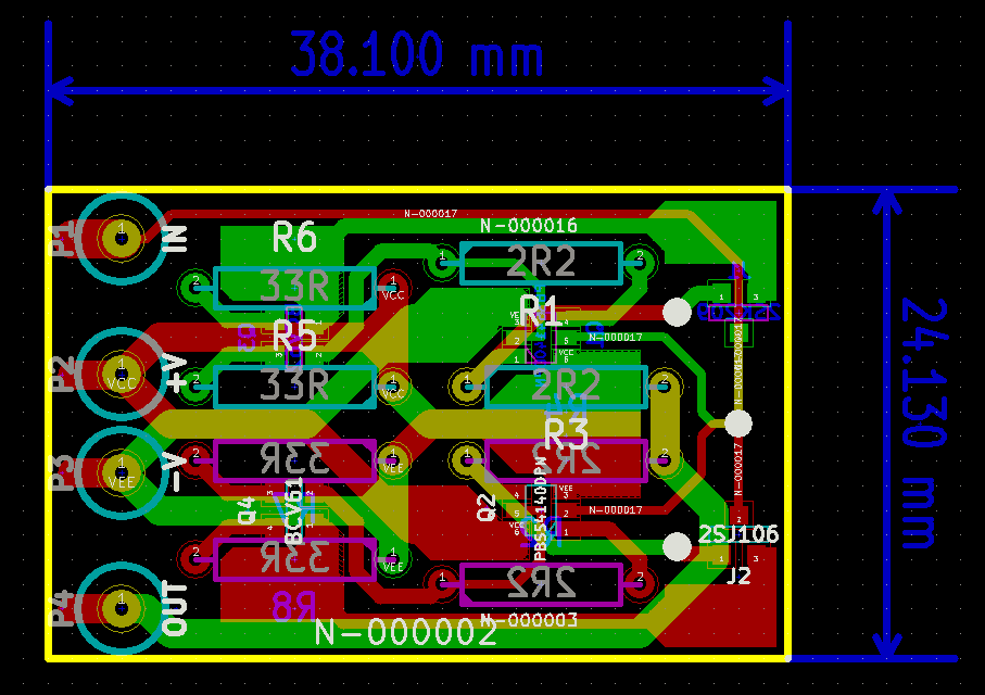
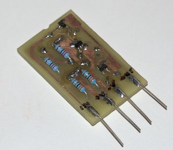
I picked up a cheap laser printer and used the toner-transfer method to make this PCB instead of hand-drawing them like I usually do. It was the first time I had tried this method, so I was pleased that it worked well.
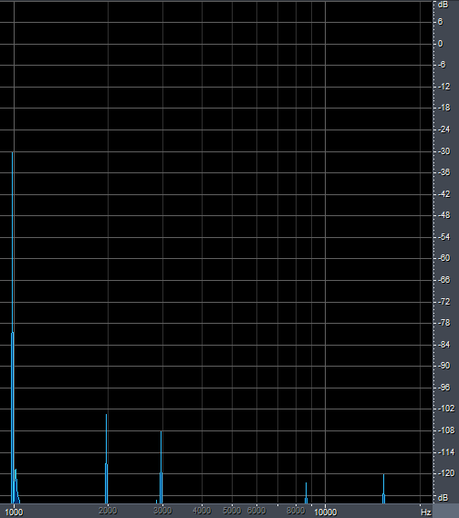
The measured performance of this circuit is excellent. The following FFT shows distortion at 1kHz, 1V output into a 1kΩ load. It works out as a THD of 0.00075%.