Phono Preamplifier
I almost never listen to it, but I do have a turntable hanging around and it needs a preamp. So I have designed this RIAA circuit. There are a few notable features: It is made from JFETs because I purchased a lot recently and like them a lot; It has no global negative feedback, although I generally advocate copious use of NFB I thought I'd try something a little different this time; the RIAA equalization is split in two and applied between the legs of long-tailed pairs (i.e. it is feedback applied between two outputs rather than from output to input, as is usual).
Single Ended
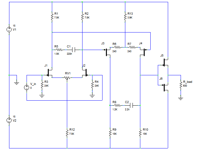
This is the basic circuit. J1/2 are 2SK389 monolithic dual JFETs and J3/4 are the complementary 2SJ109. These are used for excellent pair matching and low noise. J5/6 are 2SK170/2SJ74, but almost any pair of JFETs will do there.
J1/2 form the first LTP. It's a balanced input to help common-mode rejection. RV1 adjusts the DC offset, which is essential to maintain zero DC at the output in the absence of global NFB and the balance also strongly affects the equalization (offset will vary the effective values of the load resistors). The value of RV1 is 500Ω, but depending on the gain of the JFETs it may need to be higher or lower, since it determines the gain of the LTP (by applying local NFB). It should definitely be of the multi-turn type for accurate setting. R1/2 and C1 form the first pole at 50Hz. R5 and C1 the zero at 500Hz.
J3/4 form the second LTP. The values of the tail and load resistors have been chosen so that DC offset is (ideally) zero with ±15V supply voltage. R6/7 apply source degeneration, like RV1 in the first LTP, to reduce the gain down to the desired value. Again, depending on the gain of the JFETs the exact values needed may be higher or lower. R9/10 and C2 form the pole at 2122Hz. There is also an extra zero formed by R8 and C2 at 50kHz. I have seen this extra zero suggested to compensate for the finite gain applied during recording, which makes sense.
J5/6 are simply a source follower, buffering the output to prevent the equalization being affected by the input impedance of whatever circuit follows.
When properly balanced it is within about ±1dB of the RIAA curve. Distortion is pretty low. DC offset is stable, but I would recommend using it only with an amp with an AC coupled input, just in case something happens.
Note that the circuit does not have very good PSRR, so a low-noise regulated power supply is highly desirable. Note also that using current sources in the tails of the LTPs instead of resistors will not help here. In fact it will make PSRR worse, since with the resistors there is partial cancellation of supply variations between the two LTPs.
Balanced
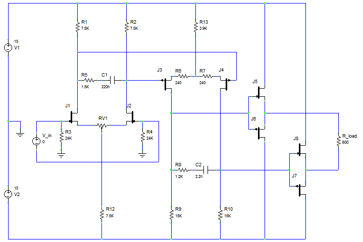
In the first circuit, there are two outputs from the second differential, but only one is used, wasting half the gain. By adding a second source-follower it is possible to have a balanced output, doubling the gain, reducing distortion and greatly improving PSRR. Obviously this is only useful if the following stage has a differential input.
Alternative balanced
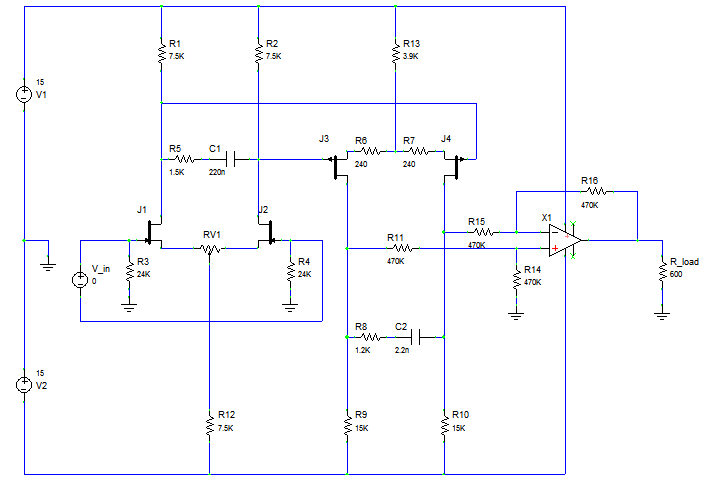
Another possibility is to take the balanced output and convert it to single-ended. Here this is accomplished with an op-amp configured as a differential amplifier.