LED driver
My desk is poorly illuminated at night and I happened to have obtained some white LEDs, so I used the one to fix the other. I decided to drive the LEDs with a switching regulator instead of a linear current source, just to see what sort of efficiency I could get. Efficiency is not really a requirement, it's just for fun.
Schematic
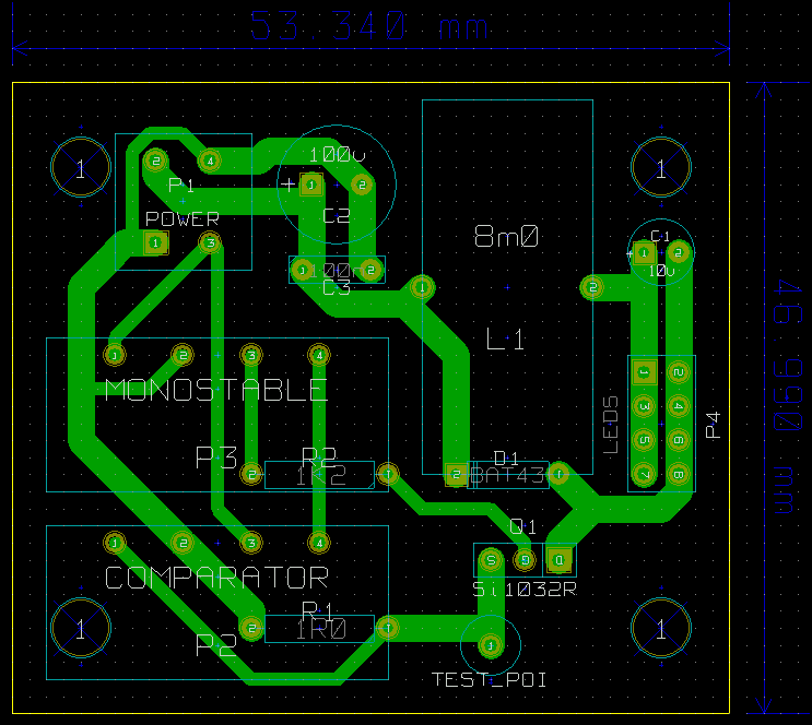
The circuit is divided into four parts: The main switching circuit, a comparator, a monostable multivibrator and the PSU. The first schematic shows how they connect together.
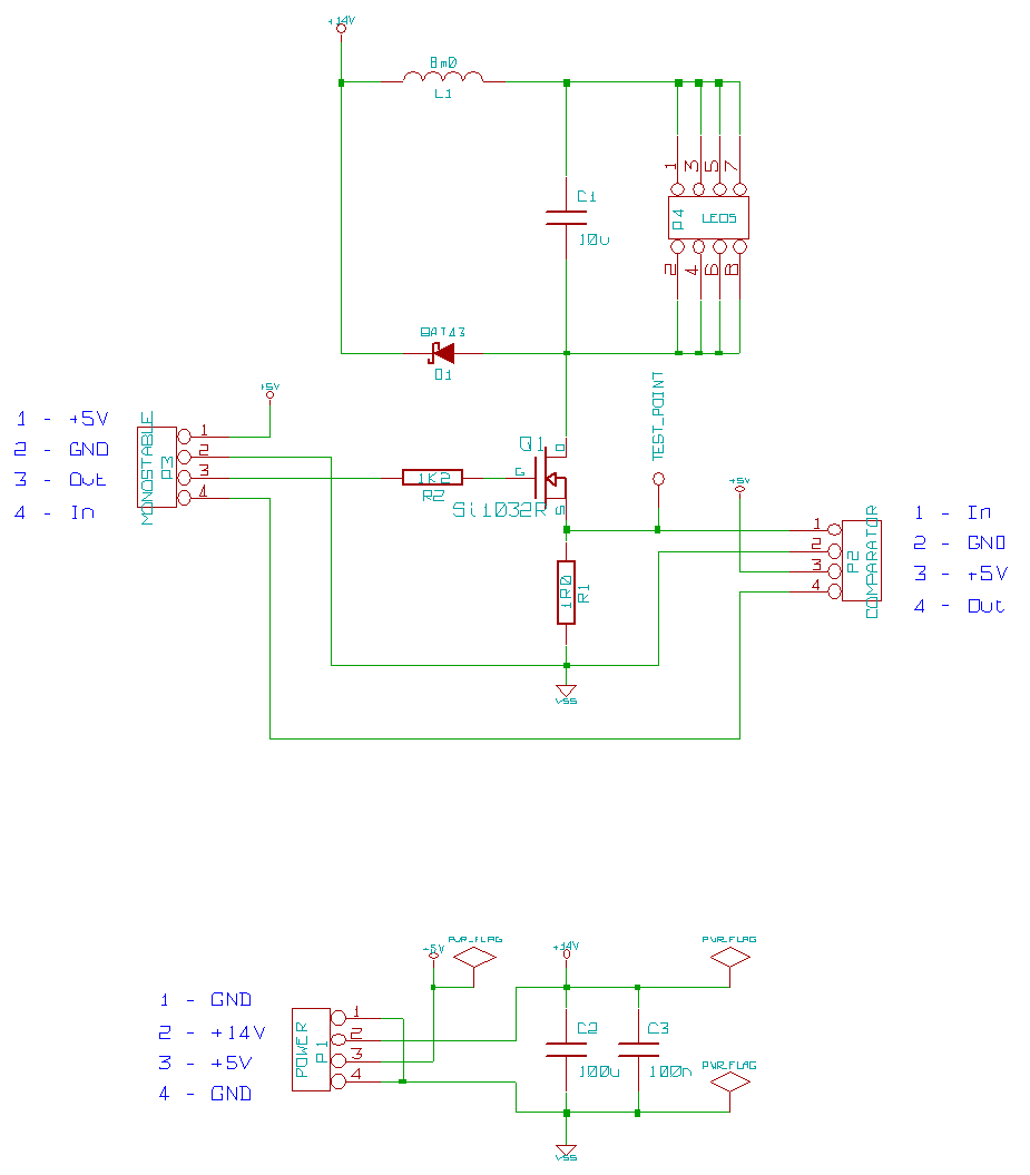
I chose a buck converter topology as it has high efficiency and the required output voltage (13V for four LEDs in series) is lower than the input voltage (14V from the transformer I used). Unlike the standard arrangement, this circuit uses a low-side switch, which is easier to drive than the usual high-side switch. This has the disadvantage that the load is not ground-referenced, but that doesn't matter for the purpose of driving LEDs. The inductor L1, MOSFET Q1 and diode D1 form the buck converter. The additional filter capacitor, C1, reduces the ripple current through the LEDs, which hopefully reduces EMI emissions a bit.
The inductor is quite big at 8mH. The large value allows for a slower switching frequency, which reduces the speed required of the rest of the circuit and reduces switching losses.
The 1Ω resistor, R1, is for current sensing. A voltage develops across it when the MOSFET is switched on, and this voltage is measured by the comparator...
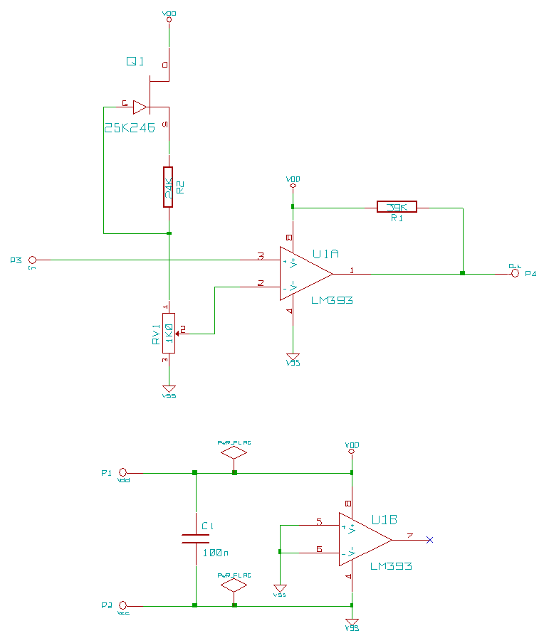
The comparator is very simple. There is a reference voltage across RV1, fed by a constant current from Q1. When the input voltage exceeds the reference voltage, the output goes high. R1 is a pull-up resistor, needed because the comparator has an open-collector output. A push-pull output comparator would have been faster, but I didn't have one available. Also, it's a dual comparator but only one is used, so the inputs of the second one are grounded to prevent it from flapping about uncontrollably.
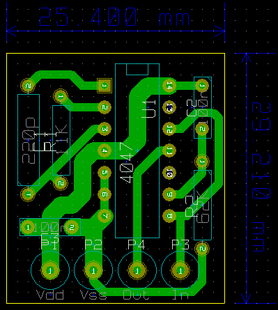
The output of the comparator is fed into the monostable...
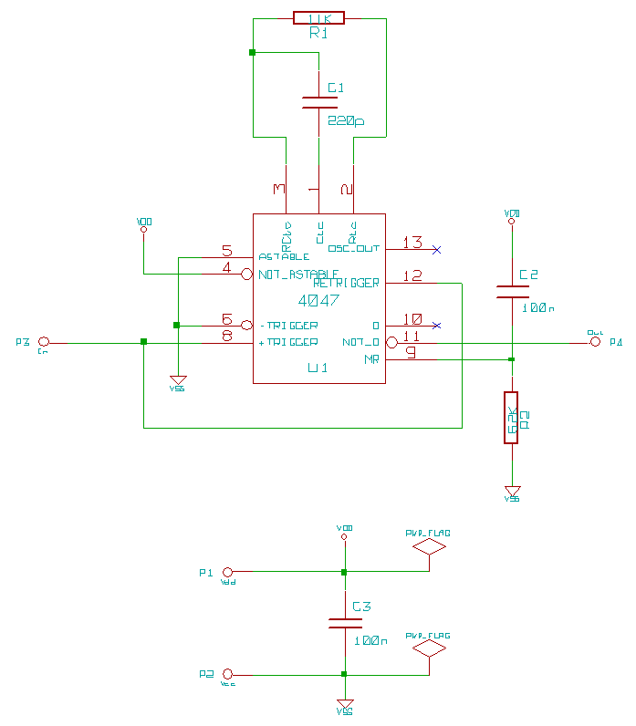
The monostable multivibrator is made from the rather useful 4047 IC. It needs only one capacitor and one resistor to work, R1 and C1 in this case, which determine the width of the output pulse.
When the comparator output goes high, the inverting output of the 4047, NOT_Q, goes low for a fixed amount of time (about 6μs), turning the switching MOSFET off, allowing the inductor to discharge. It then switches back on and the current through the inductor increases again until the comparator trips, and so on.
C2 and R2 are there because the initial state of the 4047 on power-on is not defined. If it were to start up with NOT_Q low, the MOSFET would never switch on and nothing would happen. R2/C2 hold the chip in reset long enough for the supply voltage to stabilize, ensuring that NOT_Q goes high. In practice it still occasionally failed to start, so I soldered an extra capacitor across C2 to increase its value up to about 500nF. A circuit to provide a better pulse to reset the device would be a good improvement if I were to do it again.
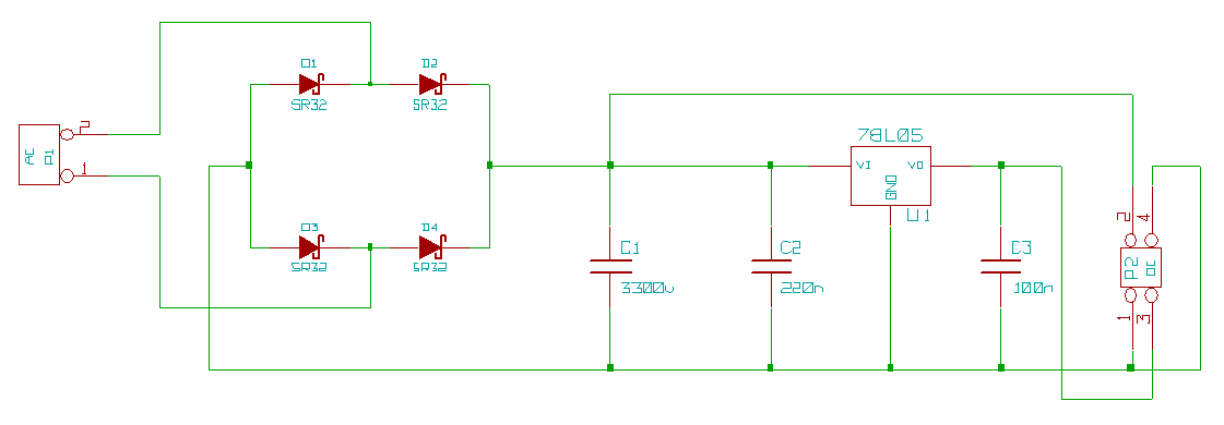
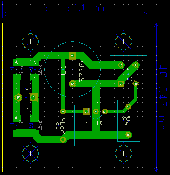
The PSU is nothing out of the ordinary, just a full-wave rectifier and reservoir capacitor. I used schottky diodes to keep efficiency up. There is also a 5V regulator to power the digital circuitry.
PCB layout
There is one PCB for each part of the circuit, plus the MOSFET is on its own tiny PCB because the Si1032R MOSFET comes in an incredibly tiny SOT-416 package and I didn't want to end up with lifted tracks on the main PCB if I failed to solder it first time. I don't recommend using such miniscule components unless you are good at SMT work!
The inductor is made from a large ferrite core that use to be part of a mains filter. It needed about 80 turns to reach 8mH, with a resistance of about 0.3 ohms. Note the pin connected to the current sensing resistor, to allow easy measurements. I should have put one the other side of the resistor too, but somehow forgot.
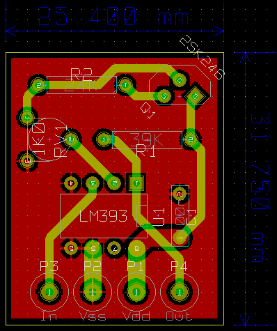
The comparator is the only one to need a double-sided PCB, which is a bit annoying as it isn't a very complicated circuit, just somehow awkward to lay out. The numbering of the pins on this and the monostable's PCBs are mixed up slightly, not corresponding to the numbers on the main PCB, but they are in the right place.
Photographs
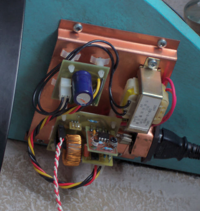
A copper plate serves to hold everything together. There is no cover, as I thought it might be nice to leave the circuit visible. In the first photo, on the plate you can see the main circuit with comparator and monostable boards attached at the bottom of the picture. The PSU is top-left, with its transformer top-right. The whole lot is mounted out of the way underneath a shelf.
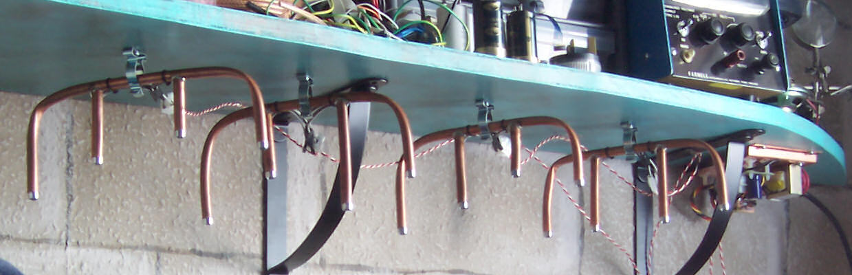
The second photo shows the strings of LEDs. There are four LEDs in series per string, mounted in chrome-plated reflectors in the ends of copper pipes held under a shelf with steel clips. I don't have a proper pipe-bender so there are a few kinks, but it looks ok. The pipes are deliberately of random lengths, in case you were thinking I just can't measure!
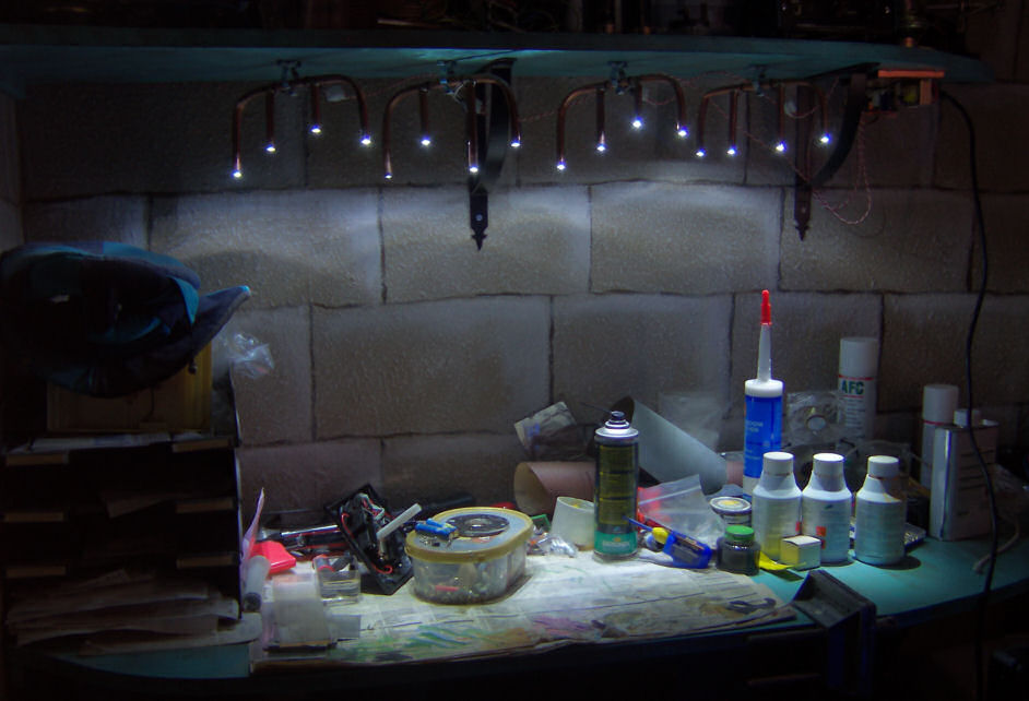
Lastly a photo of it switched on, making my desk look messy. The current through the LEDs is set to a peak of 70mA, which gives an average current of about 60mA, or 15mA per string. Even with 16 LEDs it's not particularly bright, but it is bright enough to work by.
Measurements
Since I chose a switch-mode circuit in order to learn more about them, I spent some time measuring various things. First of all, the efficiency of the buck converter itself, excluding the digital circuitry, was measured at approximately 97%, which is pretty good. The digital circuitry is not particularly low-power, so it takes the efficiency down a percent or so. The 5V regulator also wastes quite a bit.
Below is a graph of simulated MOSFET current versus time. You can see it ramping up linearly as the inductor charges up, then it drops to 0 when the MOSFET is turned off, then it rises sharply up to whatever the inductor current dropped to meanwhile.
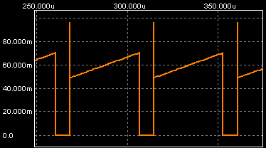
Or at least that is all it is supposed to do. In reality there is a sharp spike on the rising edge of almost 100mA, caused in the simulation by a 22pF capacitor in parallel with the inductor. The source of this capacitance in the real circuit is partly the interwinding capacitance of the inductor itself (the large size of the inductor doesn't help here), partly the capacitance of the diode and partly stray capacitance on the PCB. The spike is too quick to have any effect on the operation of the circuit, but it is a potential source of EMI. The relatively large size of the gate stopper resistor (1.2K) helps limit the size of the spike by slowing down the turn-on time of the MOSFET. Slowing it further would adversely affect the efficiency.