DC Electronic Load
Recently I have had a need to perform measurements that were time-consuming to set up, or otherwise tedious to perform with the equipment I had. Things like measuring the I-V curve of a solar panel, or the capacity of a battery, all of which involve drawing a specific current from a device and measuring the resulting voltage, either over time, or over a range of currents. That's exactly what an electronic load does - a relatively uncommon bit of kit. As usual, I came up with a list of features I wanted that don't seem to exist in commercial products, so I made my own.
The features I wanted that I couldn't find include:
- Remote control via WiFi, so I can e.g. connect it to a solar panel that's outside in the sun while I control it from inside.
- Cross-platform, so I can control it from my PC or my phone.
- Graphical display of results, to get a quick view of curves without having to export the data.
And other, more common things I wanted:
- Constant current and constant voltage modes.
- 10A, 50V (not necessarily at the same time).
- Programmable.
- Remote voltage sensing (required for accuracy at high currents).
Hardware
Having already used one for a previous project, a Raspberry Pi was the obvious choice to build it around. They come with WiFi built in, and have plenty of peripherals available, specifically a touchscreen, DACs, ADCs, and GPIO to control it all. All that digital stuff comes later though. The first thing to do was to create the analogue circuitry that lies at the heart. It's fairly simple, consisting of a single large transistor controlled by an amplifier with feedback connected for either constant current or constant voltage operation. Constant power and constant resistance modes are also possible, but I didn't implement those as I have no use for them.

The above schematic looks somewhat more complicated at first than it really is, because it's two circuits squished together. The first one is the constant current part, consisting of the op-amp U1A, MOSFET Q1, the sense resistor R5, and various other resistors. The second one is the constant voltage part, consisting of U1A, Q1, and more resistors. Which one of those two is operating is determined by the mode pins J3, which are connected to the op-amps' shutdown pins. Note that Q1 is shared, to save having to buy two large transistors. This is possible because when one of the op-amps is in shutdown mode, its output impedance is high, allowing the other op-amp full control. Additionally, the base stopper resistors R3 and R11 are sized larger than they would otherwise need to be, so that if something goes wrong and both op-amps are turned on at the same time, they won't short each other.
I selected the TLV2373 op-amp for this, as it has the required shutdown pins. It also has rail-to-rail inputs and decently low offset voltage, so it can take feedback directly from the sense resistor that is connected to ground. On testing, it turned out that even a very small DC offset was too much, so I added the potentiometer RV1 to allow the offset to be adjusted. The constant-voltage side doesn't need offset adjustment because it doesn't need to measure voltages of only a few mV above ground.
The main transistor is an IRFP7530, which is a superb example of modern semiconductor technology, having an RDSon of only 2mΩ, which is so small that it would be swamped by the resistance of the wiring. It's a bit higher than that with the 5V gate voltage it's being driven by here, but still very small. This allows the electronic load to draw its maximum current down to very low voltages.
The current sense resistor is also important. It needs to be as small as possible to dissipate as little power as possible, as the more it heats up, the more its temperature dependence will affect the measurements. It also needs to be small so that it doesn't drop too much voltage, which would limit the minimum voltage possible at high currents. On the other hand, the smaller it is, the worse the signal-to-noise ratio. I decided to go with a very small 10mΩ.

I just about managed to fit it all neatly onto a single-sided PCB. It would have been easier if I could have obtained the through-hole version of the TLV2373, but after waiting for more than a month for them to become available, I gave up and got a surface-mount one. I tried to get the feedback connection to the sense resistors away from the high-current traces, Kelvin-style. It's not quite perfect, but that doesn't matter too much, as any linear errors can be calibrated out in software.
Next is the interface, which holds the DAC that converts the digital output from the Pi into a voltage that controls the current/voltage of the electronic load, and the ADC that lets the Pi read the actual voltage/current, along with a pair of amplifiers to change the sensed voltage/current to the right range for the ADC.

The schematic is very simple because it's little more than a container for the DAC and ADC which come on their own PCBs and plug in to the interface board. Note that the amplifiers for measuring current/voltage are both differential. Even though theoretically one end is ground, and so single-ended amplifiers are sufficient, in practice the resistance of the PCB tracks and wiring is high enough that the low side of the load will be slightly above ground.
I chose the TLV272 for the sense amplifiers as they are rail-to-rail op-amps that I already had. I didn't add any DC offset adjustment for these, but I probably should have, to improve accuracy. The ADC is an ADS1115, available already on a PCB, which is helpful as they would be hard to solder by hand. It's 16-bit, which gives plenty of resolution. Likewise, the MCP4725 DAC is ready-made on a PCB. It's only 12-bit, but that's still enough to give about 2mA resolution over the full 10A range.

Not shown are a couple of capacitors across R4 and R2. I added those after noticing a large spike of interference picked up by the current sensor at exactly 1 minute intervals, coming from the WiFi. It is of course not possible to shield the WiFi and still have it work, nor is it practical to shield the analogue circuitry sufficiently, so I mitigated it by reducing the amplifier's bandwidth with capacitors. I should probably have done that from the start, since the bandwidth is far higher than needed for the modest sample rate of the ADC, which means excess noise.
The last analogue part is the power supply. It seemed sensible to run all the analogue circuitry from 5V, to keep all the voltages within what the DAC and ADC can handle. Since this supply voltage also serves as the reference voltage for the DAC, I used a linear regulator to provide it. The Raspberry Pi and its touchscreen also need 5V, but at much higher current, and they don't care so much about it being clean, so I used a couple of tiny switching regulators for those. All three regulators are powered by 12V from a "wall-wart".

Like the interface, this PCB is little more than some sockets for other boards to plug in to. The two switch-mode regulators are cheap ones from China, while the linear one I made myself, with the same pinout for convenience (I haven't bothered to show the schematic for that, as it's too simple). There are some other components present though: A common-mode choke and capacitor at the input, and some capacitors across the outputs of the regulators. The filter at the input is necessary to keep out noise generated by some of the lower-quality wall-warts I might use to power this. The capacitors at the output do the same for noise generated by the switching regulators, although they are not too noisy by themselves.
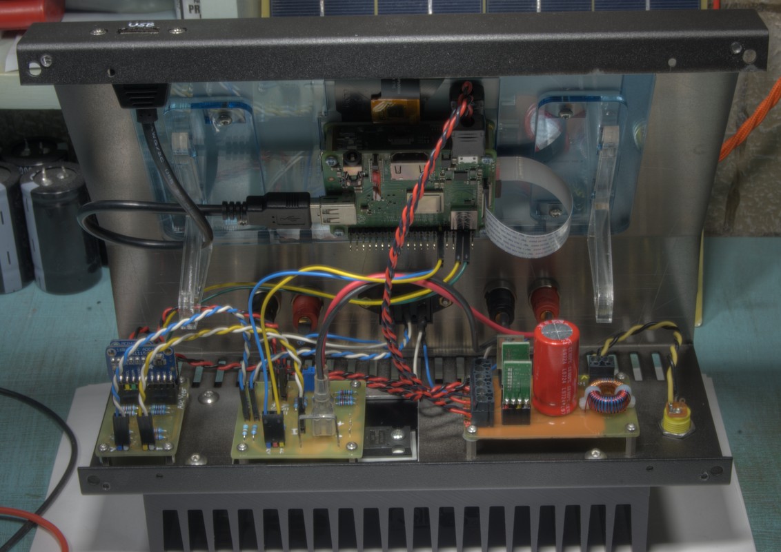
And there it all is inside the case. The two stacked PCBs at the top are the Raspberry Pi and the PCB for the touchscreen. The analogue stuff is all at the back of the case (at the bottom of the photo). On the left, the interface, then the load itself in the middle, and the power supply on the right. The main transistor is bolted to a heatsink on the back, which is big enough to handle around 100W before the transistor overheats.
Software
With the hardware assembled, I then started work on the software. As with all the other projects I've used a Pi for before, I started with WebIOPi, which has a webserver and drivers for a few I²C devices, like the DAC and ADC I'm using. Sadly it's no longer supported, and doesn't work on the newer Raspberry Pi 3, but there is a fork available, rpi3-webiopi which does work, so I used that one instead. I had to make a few modifications to it, such as adding support for more of the features of the ADS1115.
I used that to provide a simple HTTP API, exposing functionality such as turning the load on and off and setting the current/voltage. So that it can be set up and started from one device, then the results viewed on another device, it will run once started until it is told to stop or it reaches some preset limits, and it will keep all the measurements it made until asked for them (or they can be read frequently, to keep the chart updated in real time). To provide programmability, it can also accept a Python script instead of a single value for the current/voltage, which it will use to continuously adjust the load.
The client (which is just a web page) is where most of the interesting stuff happens. It has a UI for setting the voltage/ current etc. and a chart for displaying the results, which can show not only the current/voltage, but also some other values that can be calculated from those over time, such as electric charge in mAh for measuring battery capacity. Charting is done using Chartist, which is a very nicely written bit of software, if a little bare of features. The data can be exported as CSV too, so it can be further analysed elsewhere.

Above you can see the completed thing having just taken a measurement of the energy contained in a supercapacitor. The capacitor was charged up to 2.5V, then the load set up to drain it at a constant 1A until empty. You can just about see that the chart is configured to show energy in Joules, and the final value is 1377. Since the energy stored in a capacitor is E = ½ * C * V², the capacitance must be 2 * 1377 / 2.5² = 441F, which is acceptable for one that is supposed to be 500F±20%. In fact I'm pleasantly surprised, as it was a very cheap one purchased from eBay, and the manufacturer doesn't advertise anything bigger than 400F, so I was half expecting it to be fake.
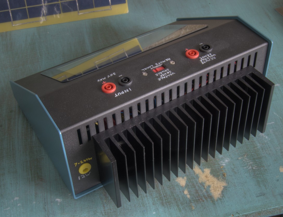
Also visible in the photo are the extra connections for remote voltage sensing. Without those, the measured voltage would be too low due to the voltage drop in the wires and connectors. There is a switch to toggle between remote sensing and local sensing (which measures the voltage from a point just inside the case). The switch is recessed so that I can't accidentally toggle it.
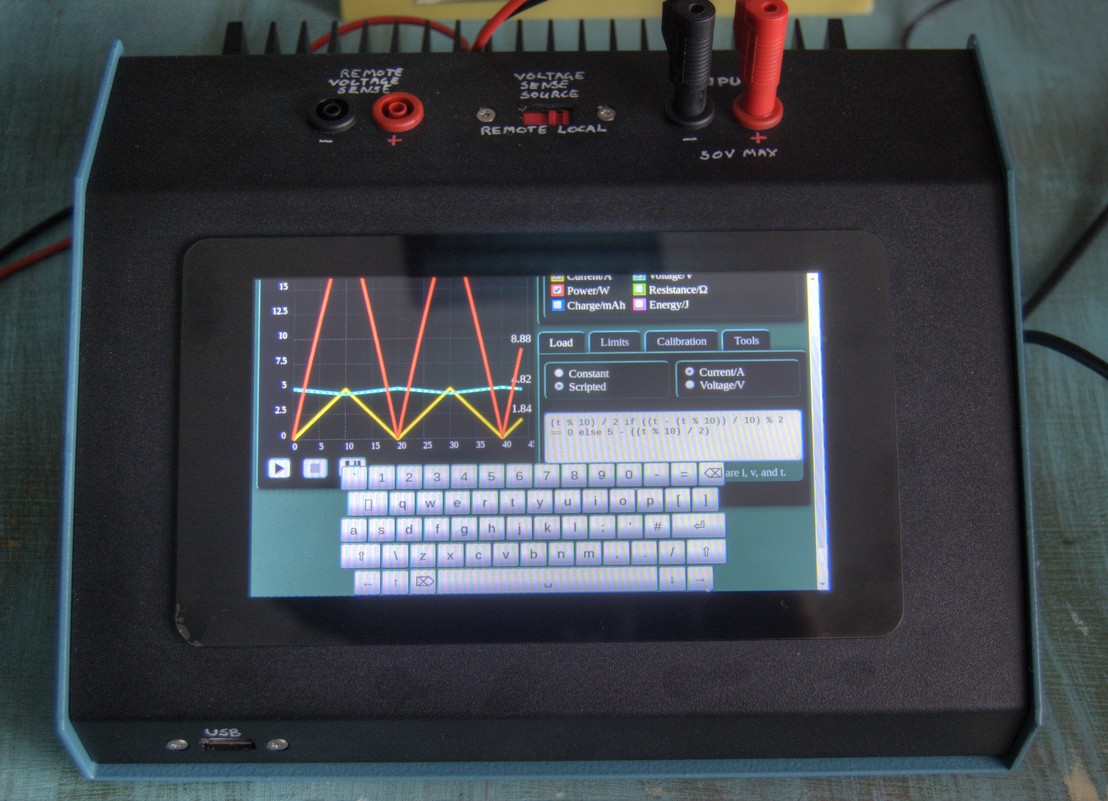
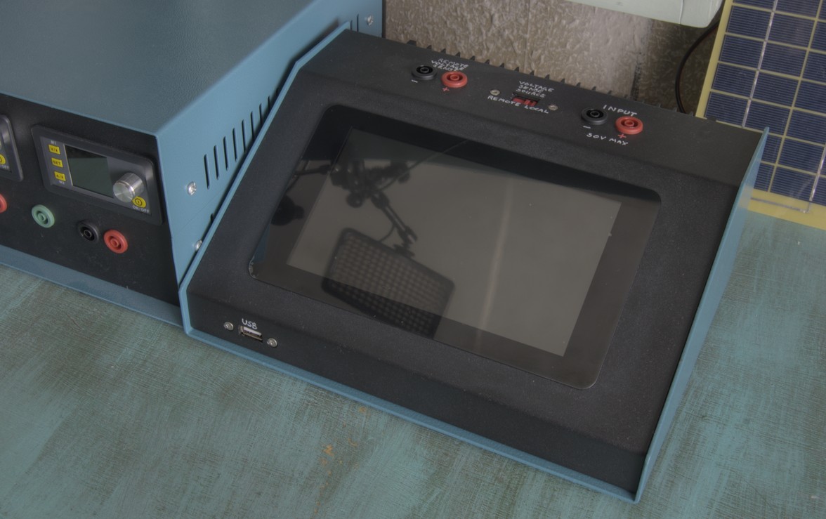
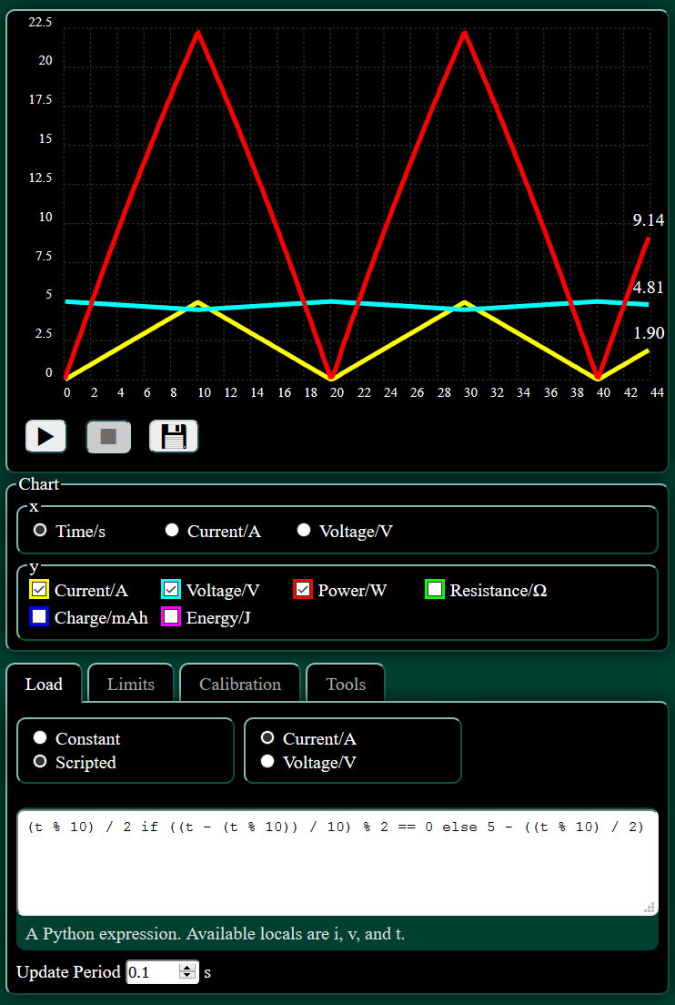
Although the Raspberry Pi has an offical touchscreen, which I used, it runs a desktop OS that lacks touchy features like an on-screen keyboard. It does have a USB port on it, which I brought out to the front panel, so a physical keyboard can be connected if required, but I really intended it to be controlled with the touchscreen alone, so I programmed an on-screen keyboard in JavaScript. It has both a small numeric keypad for entering numbers, and a full alphanumeric keyboard for text input. The above photo demonstrates the ability to use a script to control the load, in this case simply ramping the current up and down. It's hard to read the script in a photo of a small screen, so here's the same thing again as a screenshot from my PC:
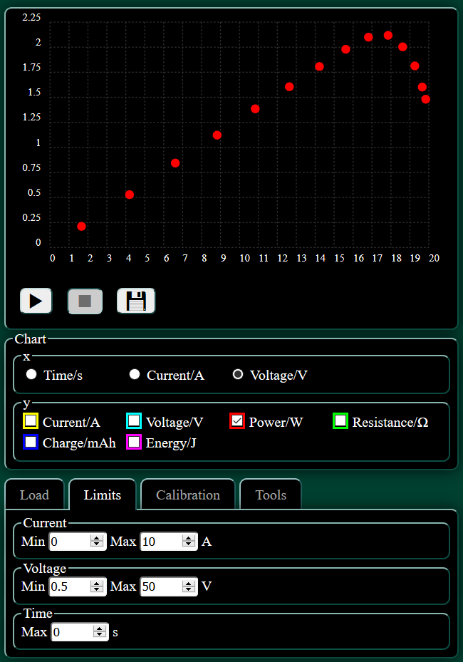
The final screenshot is a test to find the maximum power point of a solar panel. The load was set to constant voltage mode, running the script 20 - (t*t) / 10 so that it ramps down from 20V, spending more time (and thus taking more samples) at the initial higher voltages, which is the region of interest. The minimum voltage limit is set to 0.5V, which causes the load to stop once the voltage drops below that, otherwise it would run forever. The chart is set to use voltage as the x-axis and power as the y-axis, so it can easily be seen that the maximum power is achieved a little below 18V.
Source code is available both on GitHub where it's easier to browse, and as zip files here.
The modified WebIOPi that it runs on top of is also on GitHub, and here in a zip file.
Conclusion
Overall it works pretty well, doing everything I wanted it to do. There are a few shortcomings though. It has a slight problem with the temperature coefficient of the sense resistor. It's ok at currents up to an amp or so, but at higher currents the resistance slowly increases as it heats up, leading to the actual current decreasing. To completely fix that, I would need to add a temperature sensor. It's also hard to read the chart when it is displaying multiple quantities, since they all share the same y-axis, which is a limitation of Chartist. Since this is my device that I have full control over, I could work around that if I really wanted to, or add any features I might need in the future.
Mk II Improvements, March 2020
Though it worked well enough, I wanted to properly address the interference from the WiFi, and do something about what I previously thought was the sense resistor's temperature coefficient, but which a little more investigation revealed to be thermal EMF. I also took the opportunity to switch the main MOSFET for one with a wider DC SOA, so that it would be limited only by maximum power, current, and voltage.
Thermal EMF is generated by any component that is soldered to a PCB, or within a component if it consists of more than one conductive material, as the different materials form thermocouples, which convert any temperature gradient across the component into a voltage. The voltages are very small and so are not usually a problem, but since I used a very low-value sense resistor, and it was physically large enough to have a few degrees of temperature difference between its terminals, it was enough to make the measured current appear offset by many milliamps. To reduce the magnitude of the EMF, I changed the sense resistor to one that has a specified low thermal EMF, with terminals closer together, and I mounted it on the heatsink to minimize the temperature difference between the terminals. So that any remaining EMF had as little effect as possible, I used a sense resistor with a larger resistance, which yields a larger sense voltage, making the thermal EMF relatively smaller in proportion.
To reduce the WiFi interference, and lower the noise floor generally, I simply added capacitors to reduce the bandwidth of the load, and of the signals at the ADC inputs. Furthermore, as the voltage generated by the sense resistor is now larger, I was able to directly read it with the ADC instead of needing an amplifier, removing any noise generated by that amplifier.


In the interface schematic, R5 and R6 are part of the filter at the input of the ADC that measures the voltage across the load. They are significantly larger than the 1kΩ maximum that the datasheet recommends. However, since the datasheet also says that the ADC's input impedance is resistive, having larger filter resistors should only result in a linear error in the measured value, which can simply be calibrated out. Both ADC inputs are low-pass filtered at about 200Hz, which keeps out most of the noise while still allowing for fast measurements. Unlike the original circuit, the ADCs are configured to take differential measurements, as they don't have amplifiers in front to do differential to single-ended conversion.


To see how much effect on noise the filtering had, I set the load to a low current of 20mA for a couple of minutes, long enough to capture the spikes of noise from the WiFi which happen every minute, first with the original circuitry and then again with the new.

Before, the Wifi interference produced spikes large enough to appear as a peak-to-peak error of over 20mA, and the background noise was also several mA. After, the WiFi spikes have been reduced to about 2mA, and the background noise to a fraction of a mA. That should be good enough for most purposes, although I would still like to remove those spikes altogether somehow.
To test the change in thermal EMF, I programmed the load to draw 20mA for 10s to get a baseline, then 4A for 30s to heat up the sense resistor, then 20mA again to see how much offset had been added.

Before, the error immediately after the high current period was 60mA! This implies that the thermal EMF was a whopping 600µV across the 10mΩ sense resistor. After, there is no measurable error at all.
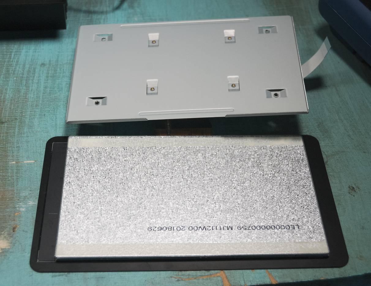
Coincidentally, the screen fell off, revealing that the metal shell on the back is only held on with sticky tape. Clearly it's not meant to be attached to a chassis in the manner that I used. I just stuck the metal bit back on with epoxy, which will be strong enough to hold it.